The roughness of any floor, except forged surfaces, could also be expressed by means of symbols and numerical ratings. The finish mark symbols are used to designate the relevant surface. The numerical rating indicates the roughness of that surface.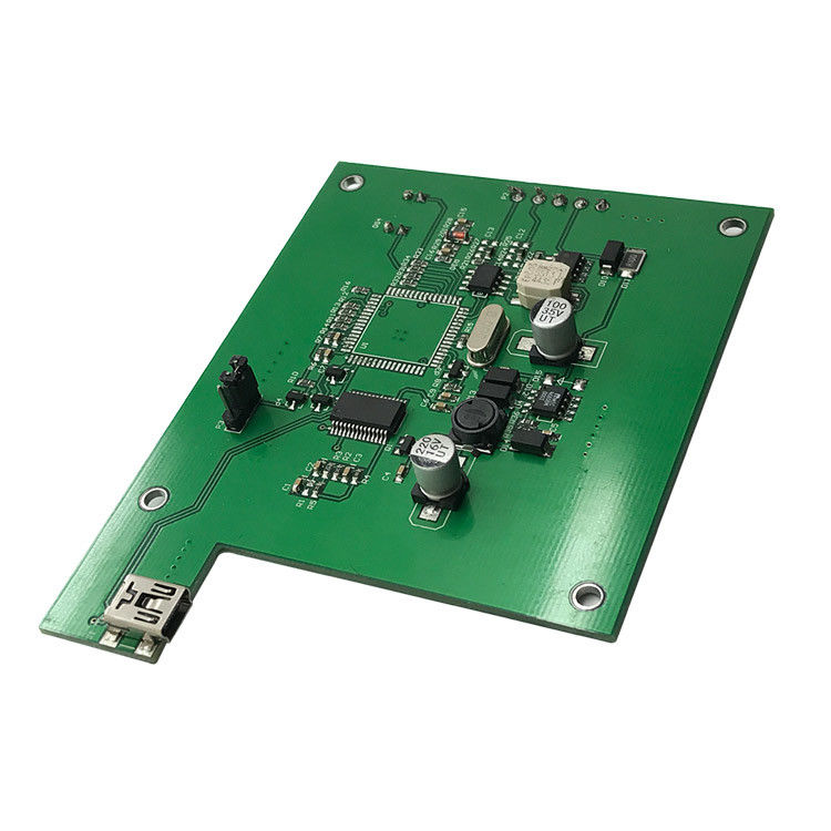 The roughness of any surface is set by design requirements relatively than by manufacturing processes: nonetheless, over control will increase the cost of production. Therefore, specify surface roughness management on drawing solely when it is essential to the looks or mechanical performance of the product. Castings: Do not use symbols. Ratings on solid surfaces. Mill Cleanup. When you loved this article and PCB you would like to receive much more information relating to PCB, Getpocket.Com, please visit our own site. Shear Cuts… 001 to .005 Tolerance… 0005 to .001 Tolerance… 0002 to .0005 Tolerance… 0000 to .0002 Tolerance… The nonconductive air house between traces, pads, conductive matter, or any combination thereof. The width of the conductor surrounding a hole by way of a Printed Circuit Pad. An precisely scaled configuration used to provide a Master Pattern. Generally prepared at an enlarged scale using varied width tapes. Special shapes to characterize conductors. American Wire Gauge. A method of specifying wire diameter. The higher the number, the smaller the diameter. Leads popping out of the ends and alongside the axis of a resistor, capacitor, or other axial part, quite than out the facet. A situation that generally occurs during the wave soldering operation where excess solder builds up and shorts out the adjoining conductors. A Heavy trace or conductive metal strip on the Printed Circuit Board used to distribute voltage, grounds, and so forth., to smaller department traces. A capacitor PCB board review used for providing a comparatively low impedance A-C patharound a circuit element. A coating that is mostly sprayed, dipped, or brushed on to offer the completedPrinted Circuit Board safety from fungus, moisture and debris. A protrusion of the Printed Circuit Board edge that’s manufactured to a configuration to mate with a receptacle that provides electrical and/or mechanical junction between the Printed Circuit Board and other circuitry. A circuit comprised of mostly integrated circuits which operates like a change (i.e., it is either «ON» or «OFF»). A part which has been fabricated prior to its set up (i.e., resistors,capacitors, diodes and transistors). A plated-through hole in a Printed Circuit Board that is used to provide electrical connection between a trace on one aspect of the Printed Circuit Board to a trace on the other aspect. Since it’s not used to mount element leads, it is generally a small gap and pad diameter. Also called wave soldering. A way of soldering Printed Circuit Boards by shifting them over a flowing wave of molten solder in a solder bath. A material used to fabricate Printed Circuit Boards. The base material (fiberglass) is impregnated with epoxy filler which then must have copper laminated to its outer surface to kind the fabric required to manufacture Printed Circuit Boards. A two-dimensional network consisting of a set of equally spaced parallel traces superimposed upon another set of equally spaced parallel lines in order that the strains of 1 set are perpendicular to the lines of the other. A condition where all unused areas (areas not consumed by traces or pads) of the Printed Circuit Board are left un-etched and tied to the ground circuit throughout the board. An precisely scaled sample which is used to supply the Printed Circuit inside the accuracy specified within the Master Drawing. Also referred to as the Back Plane, or Matrix Board. A comparatively large Printed Circuit Board on which modules, connectors, subassemblies or other Printed Circuit Boards are mounted and interconnections made by way of traces on the board.