 Printed circuit board (PCB) inspection is a critical step in making certain quality and reliability across the electronics manufacturing process. Both bare boards and assembled PCBs must be carefully examined to validate acceptability before shipment to clients. But what specific standards represent a correct PCB inspection? Read on for an summary of inspection aims, standards, metrics, tools, and key defect sorts checked in the course of the PCB inspection process. Thorough inspection in opposition to established standards minimizes shipping defective boards to customers. Manufacturers typically outline an inspection plan with accept/reject standards mapped to those requirements. If you are you looking for more info about printed circuit board article check out our own page. IPC requirements specifically provide a framework for interpreting the severity of sure defects. Tracking metrics gives knowledge to repeatedly improve processes and product quality over time. Automated Optical Inspection (AOI) – Imaging system scans boards at high decision capturing any defects. Computer algorithms analyze photos towards CAD data to detect discrepancies. Solder Mask Inspection – Validating uniformity and accuracy of solder mask application. Checking for voids, skinny areas, misregistration.
Dimensional Inspection – Measuring essential attributes like board thickness, lengths, hole positions. Confirming inside specified tolerances. Hole Wall Integrity – Testing plated through-hole conductivity and plating high quality utilizing strategies like automated flying probe electrical testing. X-Ray Imaging – Captures defects inside boards like cracks, delamination, voiding, drilling errors. Thermal Stress Testing – Subjecting boards to thermal shock, cycling, and dwells reveals latent material stresses and workmanship points by way of failure evaluation. Cross-Sectioning – Cutting micro-sections to inspect plating thickness, resin fill, glass weave, and other inside board particulars below microscope. Bare board inspection focuses on design, fabrication, and materials quality prior to parts being mounted. Bill of Materials (BOM) Accuracy – Confirming correct components installed in each designators position. Polarity – Verifying half orientation matches footprint polarity. Presence/Absence – Detecting missing elements not mounted or incorrect portions. Component Value – Validating correct nominal worth components installed like right resistor resistance or capacitor values.
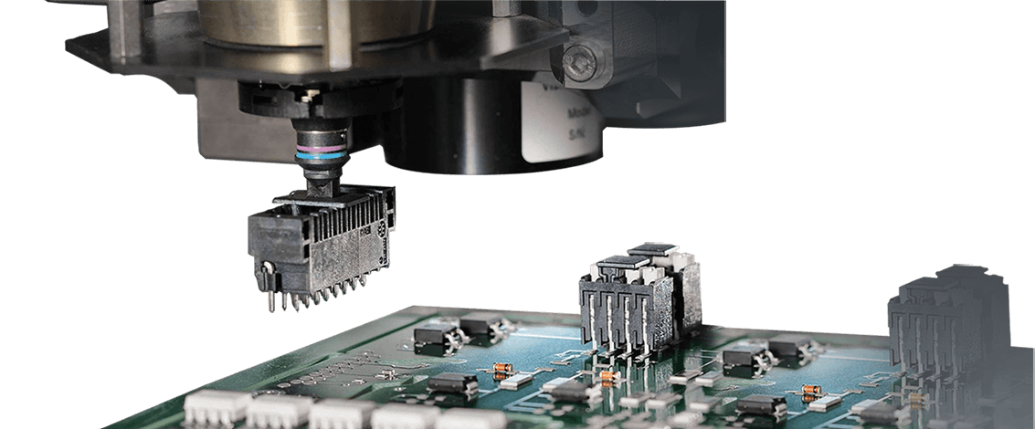
Placement Accuracy – Checking location placement precision against CAD centroid positions. Solder Joint Quality – Inspecting that solder fillets, toes, and bonds meet acceptability criteria. Foreign Object Debris (FOD) – Checking no free particles, dirt, debris, or hair exists on the assembly. Mechanical Assembly – Ensuring no bent leads, visible damage, board warpage, discoloration, or scorching. Electrical Tests – Running in-circuit assessments (ICT), boundary scans, and purposeful checks to verify proper electrical efficiency. Assembled board inspection focuses on components, soldering, and performance pre-shipment. Missing fine pitch marking. Automated Optical Inspection (AOI) – Vision cameras with refined algorithms rapidly scan boards against CAD models detecting discrepancies. Can inspect solder joints, elements, PCB features, markings, and extra. High throughput inline operation. Automated X-Ray Inspection (AXI) – X-ray imaging reveals hidden defects and confirms BOM, placement, and pcb assembly (Suggested Looking at) solder joint quality with out destructive dismantling. Especially helpful for dens chips, BGAs, and QFNs. Solder Paste Inspection (SPI) – Validates quantity, space, height uniformity, and print registration of solder paste deposits through 3D optical metrology.
In-Circuit Test (ICT) – Electrical probes test nodes throughout circuits verifying right performance. Fixtures allow repeatable probe alignment. Bed of Nails Test – Spring-loaded take a look at pins make electrical contact at testpoints across board checking continuity, shorts, and opens. Flying Probe Test – Automated probe mechanism touches down in any respect take a look at nodes in a programmed sequence with out use of a fixture for PCB board electrical verification. Automated inspection replaces manual visible checking with quick, objective, repeatable assessment against acceptance standards thresholds. Every product usually maintains a personalized checklist based mostly on vital traits and risks assessed from prior builds. What magnification is used to inspect PCBs? Solder joints, machined features, and positive pitch parts require magnification. Handheld microscopes range from 10x to over 100x. Machine vision cameras provide as much as 200x magnification. What are common PCB inspection failure points? Typical defects are skinny/inadequate solder, missing or incorrect parts, poor solder fillets, pads lifted from board, scorched areas, flexed boards, and debris inclusions.
 How does automated optical inspection (AOI) work? AOI compares pictures of board options to CAD knowledge using refined algorithms to determine discrepancies in the location, assembly, and soldering revealing any defects. Does PCB inspection impact production rate? Automated inspection integrates inline with out slowing general price. Manual inspection can develop into a bottleneck. AOI provides 10x the inspection points per hour compared to handbook. What data ought to PCB inspection reviews include? Reports convey pictures/particulars of each defect found, measurement data, defect counts, course of capability metrics, repair suggestions, and pass/fail standing relative to acceptance standards. Rigorous PCB inspection in opposition to established acceptability standards ensures high quality and reliability. Both bare boards and assembled PCBs undergo in depth automated optical, electrical, and functional verification utilizing metrics defined by requirements. Passing scrutiny throughout parameters like soldering, components, board fabrication, and electrical operation provides confidence previous to shipment. By institutionalizing strong inspection practices as a core discipline, electronics manufacturers reduce escapes, pcba (canvas.instructure.com) area failures, and guarantee customer satisfaction. It is strictly forbidden to immediately take a look at the Tv, audio, video and other equipment without energy isolation transformer with the equipment that’s grounded.